Antennas are sensitive to the surrounding environment. Therefore, when there is an antenna on the PCB, the PCB layout design should take into account the requirements of the antenna, as this may greatly affect the wireless performance of the device. Extra care should be taken when integrating antennas into a new PCB layout design. Even the material of the PCB, the number of layers, and layer thickness can affect the performance of the antenna.
What are the advantaged of PCB layout designed antenna?
PCB antennas have the advantages of simple structure, low cost, small size, and lightweight. Multi-band omnidirectional antennas with efficient printed circuit board design can be integrated into devices that require wireless functions, such as Bluetooth and Wifi, and omnidirectional radiation patterns become ideal for multi-point and mobile wireless systems.
With the development of IoT and smart hardware products, antennas are needed for networking and transmitting data. The smaller the space, the more frequency bands, and the more complex the antenna design.
Compared with an external antenna, the built-in antenna is more suitable for handheld, wearable devices, smart homes, and other small-size products with high integration to ensure the product appearance is not affected.
At present, the built-in antenna mainly has a ceramic antenna, PCB antenna, FPC/metal sheet antenna, and LDS antenna.
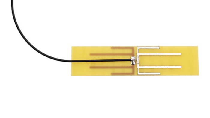
We mainly introduce a PCB layout designed antenna here. It is made by electronic printing technology, also known as a printed circuit board. For decades, with the continuous improvement of internal design, it has also been more and more widely used.
PCB layout designed antennas work in different patterns and, depending on how the individual antennas radiate, may need to be placed in specific locations – along the short side, long side, or corners of the PCB.
Usually, the corners of the PCB layout design are very good locations to place antennas. This is because the corner position allows the antenna to have clearance in five spatial directions and the antenna’s feed is located in the sixth direction.
Antenna manufacturers offer a choice of antenna PCB layout designs for different locations, so product designers can choose the antenna that best fits their layout. Often, the manufacturer’s data sheet will show a reference PCB layout design that, if followed, will provide very good performance.
Product PCB layout designs for 4G and LTE typically use multiple antennas to build MIMO systems. In such designs, where multiple antennas are used simultaneously, the antennas are usually placed at different corners of the PCB layout design.
It is important not to place any components in the near field near the antennas, as they may interfere with their performance. Therefore, the antenna specification will specify the size of the reserved area, which is the area near and around the antenna that must be kept away from metallic objects.
This will apply to each layer in the PCB. In addition, no component may be placed in this area on any layer of the board, and do not even install screws.
The antenna radiates to the ground plane, and the ground plane is related to the frequency at which the antenna operates. Therefore, it is imperative to provide the correct size and space for the ground plane of the selected antenna.
The ground plane of antenna PCB layout design
The size of the ground plane should also take into account any wires used to communicate with the equipment as well as the battery or power cord that powers the equipment. If the ground plane is properly sized, it will ensure that the cables and batteries connected to the equipment will have less impact on the antenna.
Some antennas are associated with a ground plane, which means that the PCB itself becomes the grounded part of the antenna to balance the antenna current, and the lower layer of the PCB may affect the performance of the antenna. In such cases, it is important not to place a battery or LCD near the antenna.
The manufacturer’s data sheet should always specify whether the antenna requires ground plane radiation and, if so, the size of the required ground plane. This may mean that the clearance area should surround the antenna.
Proximity to other PCB components
It is critical to keep the antenna away from other components that may interfere with the way the antenna radiates. Items to be wary of are batteries; LCD displays Metal components such as USB, HDMI, and Ethernet connectors; and noisy or high-speed switching components associated with switching power supplies.
The ideal distance between an antenna PCB layout design and another component varies depending on the height of that component. Typically, if a line is drawn at an 8-degree angle to the bottom of the antenna, the component is a safe distance from the antenna if it is located below the line.
If there are other antennas operating at similar frequencies nearby, this may cause both antennas to be detuned as they affect each other’s radiation.
We recommend mitigating this situation by isolating the antennas by at least -10 dB at frequencies up to 1 GHz and at least -20 dB at 20 GHz.
This can be accomplished by leaving a greater distance between the antennas or rotating the antennas so that they are placed 90 or 180 degrees apart from each other.
Antenna PCB layout designing transmission lines
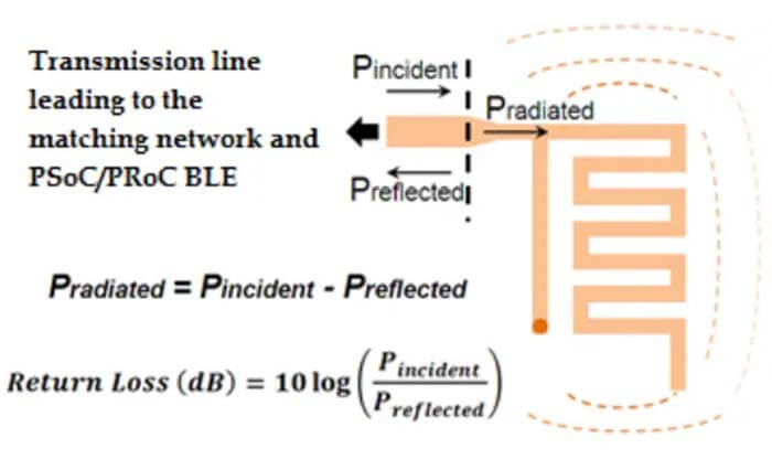
Transmission lines are RF alignments that carry RF energy to and from the antennas to deliver signals to the radio. Transmission lines need to be designed for 50, otherwise, they may reflect the signal back to the radio and cause a degradation of the signal-to-noise ratio (SNR), which may render the radio receiver useless.
Reflections are measured as voltage standing wave ratio (VSWR). A good PCB layout design will exhibit a suitable VSWR measurement, which can be measured when testing the antenna.
We recommend the PCB layout designing the transmission line carefully. First of all, the transmission line should be straight, because if it has corners or bends, it may cause losses.
Noise and signal loss that may affect the performance of the antenna can be reduced to a very low level by placing the vias evenly on both sides of the alignment, as it helps to improve performance by isolating noise propagating nearby alignments or grounding layers.
Thinner transmission lines may cause greater losses. RF matching components and the width of the transmission line should be used to adjust the antenna to operate at a characteristic impedance of 50Ω.
The size of the transmission line will affect the performance and the transmission line should be as short as possible to make the antenna perform well.
If you allow the correct ground plane and place the antenna in a very good location, you have a good start, but more can be done to improve the antenna performance. You can use a matched network to tune the antenna – this will compensate to some extent for any factors that may affect antenna performance.
The key RF components are the antenna, its matching network, and its RF output. Placing these components in a nearby configuration will minimize signal loss.
Again, if your PCB layout design includes a matched network, the antenna will perform very well if its alignment length matches the alignment length specified in the manufacturer’s product specifications.
The housing around the PCB may also vary. Antenna signals do not propagate in metal, so placing the antenna in a metal enclosure or an enclosure with metal properties will not be successful.
Likewise, be careful when placing the antenna near a plastic surface, as this can cause significant damage to the antenna performance.
Some plastics (e.g., glass-filled nylon) have losses and can attenuate the RF signal to the antenna.
Plastics have a higher dielectric constant than air, which can seriously affect the signal. This means that the antenna will record a higher dielectric constant, which increases the electrical length of the antenna and reduces the frequency radiated by the antenna.
Besides the How To Make A PCB Layout Design For An Antenna article, you may also be interested in the below articles?