PCB Antenna Design
Custom Antenna Manufacturer

PCB Antennas

Internal Antenna 4G PCB Antenna Design Manufacturer - C&T RF Antennas Inc

Embedded Antenna Design

All PCB antennas are board-specific and the dimensions and matching will need to be determined for each implementation. Copying an existing design does not ensure good performance. Gain and radiation patterns will vary as the parameters in the surrounding areas change. The length of the antenna will need to be adjusted according to these variables. Additionally, the final tuning and matching should be completed in the end product enclosure and installation, not in the open air.

​The C&T RF antennas Inc’s PCB-Based Embedded Antennas for RF solutions
The C&T RF antennas Inc’s Embedded Antennas feature a highly efficient PCB-based low profile design optimized for confined industrial designs. Ideal for embedded applications requiring integration flexibility, the Profile family includes case, through-hole, and SMT mount designs and is available in single, dual, tri-band, and multi-band applications.

Features:
1). Highly efficient PCB-based antenna solutions for ODMs and OEMs
2). Low profile embedded antenna design for confined industrial designs
3). The case, through-hole, & SMT mount designs for embedded applications requiring integration customization
4). Designed for use in WLAN, WiFi, GSM, GPRS, GPS, NB-IoT, Lora, ISM, LPD (433 MHz), Cellular LTE, and  New 5G frequency bands.

Benefits:
Stable and reliable in performances
PCB antenna has excellent sensitivity to consistently provide high signal reception efficiency
Compact size
RoHS compliance

The C&T RF antennas Inc’ embedded antenna attaches directly to the PCB and is hidden inside the product case. They’re a good fit for applications where concerns about the size, appearance, security, or environmental issues make an external antenna impractical.

How you can make the PCB/Flex PCB antenna?

  • Understand the available typical antenna kinds

Basic PCB layouts that are extensively readily available consist of the monopole, L-type, and F-type. Basic F-type antennas are one of the most thoroughly made use of, and supply the greatest trade-off in between dimension, performance, and are relatively omnidirectional. A meandering map can surely be made use of to portable the PCB location, however, this will go to set you back on efficiency.

  • Take into consideration the Building of your Circuit Board

The PCB map size will figure out the resonant frequency; the greater the regularity the much shorter the map. Each antenna needs a keep-out location on the PCB. This is specified as a location about the antenna map where no copper traces or ground load can surely be made use of on any kind of layer of the PCB.
Bigger traces are frequently much far better, as they generally offer a larger data transfer. The map can surely either be gold flashed or protected with a solder mask. The antenna’s electric efficiency will be established by the substratum product made use of, its density, and its dielectric consistency (εR).

  • The Ground Airaircraft is Vital!

PCB map antennas are ground air aircraft reliant, as they should have actually a ground air aircraft to work. The form and dimension of the ground air aircraft about the antenna will impact the insusceptibility and efficiency of the PCB antenna. The ground air aircraft ought to have actually vias along the whole side of the antenna keep-out
location.

The fundamental treatment appears like this:

Choice an IC

Check out the Datasheet of your chip, locate the instance design area

Does your application have actually physical dimension constraints? Does your Antenna need to be directional?

Utilize the solution to the over concerns to pick your antenna kind (whip, cable, chip, PCB trace)

Make your PCB design based upon the instance design. Dimension the feedline for your application

Develop some boards

Examination the antenna with an SMA adapter and a range analyzer, when possible. (in your room if you are utilizing one)

Utilize your screening result in proper your make

Built-in Antenna 4G LTE Antenna Design Manufacturer - C&T RF Antennas Inc

Your PCB Antenna Manufacturer

Why focus on PCB antennas?

In the vast landscape of IoT sensor technologies, protocols, vendor-specific SoCs and development boards, antennas, link budgets, and integrity of the wireless link between nodes are often overlooked.
Most IoT devices use whip antennas, PCBs, or chip antennas, with The specific antenna is usually determined by an omnidirectional directional map with a specific vertical/horizontal beamwidth.
If a specific edge device must be connected, a directional antenna (e.g., Yagi) may be used. directional antennas (e.g., Yagi) are used to extend the range. Each antenna type has its own advantages and considerations.
PCB antennas are efficient because of the balance between gain and size. be configured inside the housing rather than sticking out like a representative whip antenna.
Unlike chip antennas, PCB antennas can operate at a relatively high gain over a relatively large bandwidth.
During manufacturing, PCB antennas can even be embedded into system-level boards to achieve a smaller device size.
In addition to the substrate surface, antenna design and placement may also need to focus on the integrity of the link one-by-one radiation quality will be directly affected by the adjacent electronic components, metal enclosure hardware, and the quality of the antenna. adjacent electronic components, metal enclosure hardware, and environmental interference.
When trying to improve the link budget, it is important to consider the transmit/receive antenna gain, free-space path loss at a given carrier frequency, antenna feed loss, transmitter and receiver loss, and various environmental losses and other factors.
However, regardless of the environment, the directional map, gain, VSWR, and bandwidth are all parameters that are initially evaluated in the first step of wireless link development and optimization. However, regardless of the environment, the directional map, gain, VSWR, and bandwidth are all parameters that are initially evaluated in the first step of wireless connection development and optimization.

Your PCB Antenna Manufacturer

Understanding common PCB antenna designs

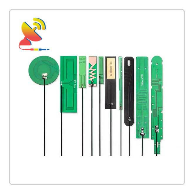
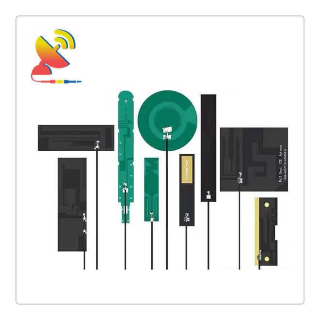
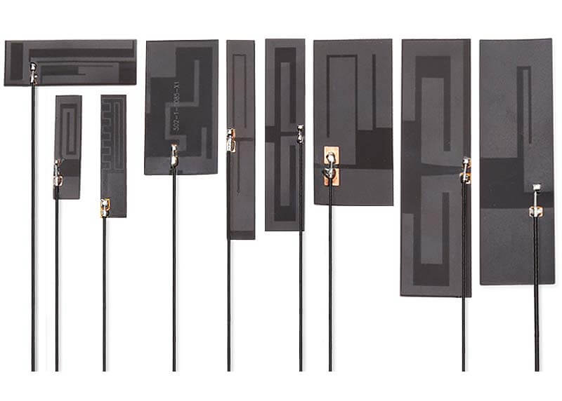
PCB antenna structures can be monopole, dipole, slot, patch, and planar inverted F (PIFA).

Dipole and monopole antennas

Dipole antennas consist of two quarter-wavelength (N/4) long metal strips with a total electrical length required to be half a wavelength (N2) below the carrier frequency for maximum response.
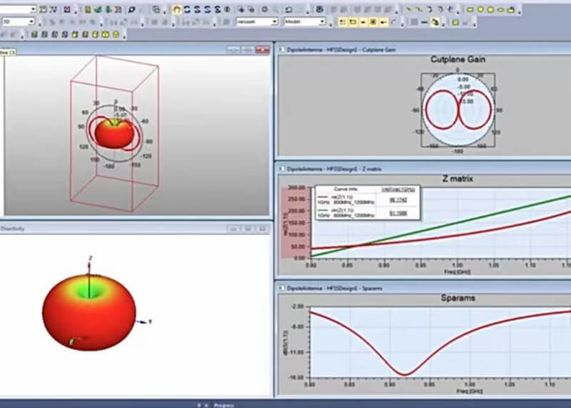
Due to the widespread use of legacy protocols such as Bluetooth and Wi-Fi, much of the antenna literature focuses on antenna design in the 2.4 GHz ISM band. At 2.4 GHz, the length of the dipole antenna is about 6 cm, which may be too large for some applications. The omnidirectional radiation direction map has a concentrated electromagnetic energy perpendicular to its length (z-axis) with a zero point in the middle (along the z-axis).
This usually requires placement in the vertical direction to obtain maximum horizontal summer coverage one by one for designers intending to use dipole (or monopole) antennas in IoT devices, which is a cause for careful consideration.
The addition of a grounding element eliminates one arm of the dipole, resulting in a structure that includes a single quarter-wavelength conducting element with the grounding element acting as the other quarter-wavelength arm.
Similar to a mirror, the grounding element generates a virtual image of the same directional map (same direction and phase of current flow) as the conducting element.
In order for the grounding element to function optimally, it must be guaranteed to be much larger than half a wavelength. A finite grounding element leads to edge diffraction of the radiated wave, which causes the electromagnetic energy to move radially outward from the edge and leak behind the grounding element.
Ideally, for a perceptually infinite ground element, the gain of a quarter-wavelength monopole antenna should be twice that of a half-wavelength dipole antenna, because the ground element radiates only to the area above it.
This will lead to the formation of some degree of lift direction map. Again, create a zero point along the length of the conducting quarter-wavelength element (z-axis) to show the desired vertical orientation.

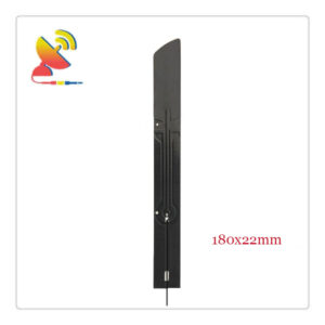
Bending monopole antennas

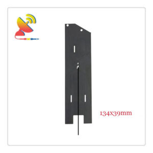
The bent monopole variants of L-shaped (or tilted whip and inverted L), planar inverted F (PIFA) and zigzag inverted F (MIFA) structures utilize the same grounding element and conducting arm approach, but with a different conducting arm pattern.
The bending of the alignment allows for more compact dimensions as well as a reduction in the zero point in the radiation direction diagram.
However, in these designs, the antenna alignment usually cannot be too close to the ground, which would cause the antenna to act as a transmission line without any radiation.
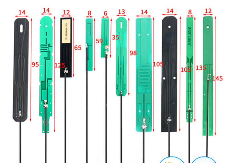
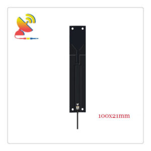
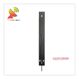
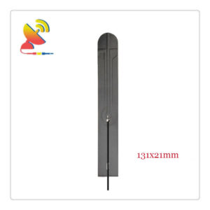
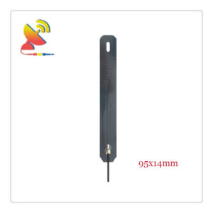
Among these variants, PIFA is the most common because of its smaller PCB area and wide bandwidth performance.
The PIFA has a fold on the main resonant line which introduces a capacitance that is offset by a short-circuit feed point at the end of the line.
Matching impedance to the antenna feed source is obtained by adjusting the lengths of A, B, and C, where A and C are sized to benefit the quarter-wavelength element, and B is adjusted for matching impedance. An external matching network can also be incorporated for additional adjustment.
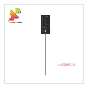
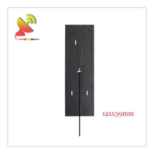
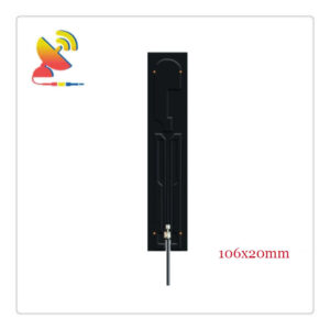
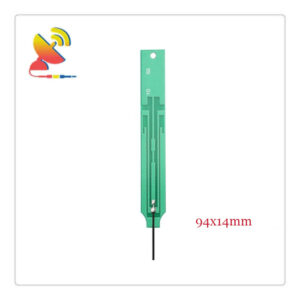
The MIFA antenna increases the total length and resonates through different directions of alignment/line compression, thus resembling a spiral antenna. In MIFA, the horizontal and vertical lines form multiple turns.
As with PIFA, tuning is accomplished by adjusting the geometry within the zigzag lines. This effectively reduces the size of the antenna.
However, there are advantages and disadvantages, and other aspects may be affected, such as reduced gain and consequently reduced range, increased tuning dependence and consequently narrower bandwidth, and increased sensitivity to interference from external sources as well as local electronics on the board.

Dipole Antenna Variants

Printed dipole antennas mainly face a size disadvantage. This is especially relevant for low frequencies;
Here, the advantage of a monopole antenna element is its potential placement in a corner of the board, where the grounding element is used both as an RF ground plane/return path for the antenna and as a grounding element for the local electrical components of the crop networking module.
However, as the operating frequency increases, this disadvantage becomes less prominent.
In addition, different dipole patterns can be used to increase bandwidth and reduce the size as with bent monopole antenna structures.
Making the dipole arm gradually narrower is a known bandwidth enhancement technique.
For example, the plane tapered dipole antenna (also known as butterfly antenna) behaves as a uniform tapered transmission line. When the RF signal is applied to the feed source, the current will flow radially outward and form a closed magnetic field.
The current terminates abruptly at the edge of the butterfly, resulting in more reflections and narrower widths compared to its 3D biconical shape.
Nevertheless, the antenna can achieve relatively constant impedance and gain over a large frequency range relative to other dipole antennas.
Along the same line of reasoning found in the bent monopole quarter-wavelength antenna, a smaller form factor can be obtained by bending the conducting arm of the dipole element.
As mentioned earlier, this optimizes the Q but reduces the overall bandwidth and efficiency. Therefore, the use of self-resonant space-saving techniques (e.g., spiral or bent conductive arms) in applications must be weighed against the pros and cons.

World's Fastest PCB Antenna Design Manufacturer

C&T RF Antennas Manufacturer

C&T RF Antennas Inc is a leading RF antenna designer and manufacturer of professional communication products including antennas, cable assemblies.
C&T RF Antennas manufacturer’s philosophy is to manufacture exceptional products with the highest quality components to assure customer satisfaction.
C&T RF Antennas manufacturer internal quality assurance programs have allowed C&T RF Antennas manufacturer to become ISO 9001:2008 certified.
C&T RF Antennas manufacturer onsite engineering department allows them to design, develop and test new products for everyone from the OEM industry to the home amateur radio operator.
C&T RF Antennas manufacturer’s house packaging allows them to private label products for C&T RF antenna customers.
Let C&T RF Antennas manufacturer help you with your professional communication needs.

Technology

Schedule on the fly

C&T RF Antennas Inc provides the fast antenna design and antenna manufacturing.

Senior Designers

C&T RF Antennas Inc has 5 senior designers and A highly skilled technical team.

High Reputation

C&T RF Antennas Inc is doing win-win business with customers based on the high reputation.

Quick Reply Within 12 Hours

C&T RF Antennas Inc sales team will respone your message within 12 hours after you drop us.

Our Services

4g lte pcb antennas manufacturer

C&T RF Antennas Inc manufactures PCB antennas with various frequency bands.

PCB ANTENNAS

FPC Antennas Manufacturer

C&T RF Antennas Inc manufactures FPC antennas with various frequency bands.

FPC ANTENNAS

Antenna Design Antenna simulation

C&T RF Antennas Inc provides embedded antennas design and customization.

ANTENNA DESIGN

C&T RF Antennas Inc is the PCB antenna and Flexible PCB / FPC Antennas designer & manufacturer in China.

About us

C&T RF Antennas Inc is the leading internal antennas and external antennas manufacturer.

Our mission

Spend a small amount of money to make your product transmit farther and maximize the value.

The Newest Antenna Products

The Newest Articles