This article introduces the 20 most effective PCB design rules in the use of design software for PCB layout design and commercial manufacturing that should be kept in mind and practiced.
Currently, semiconductor integration is increasing, many applications have readily available system-on-a-chip and are powerful, but many applications using case electronics still require the use of custom PCBs, so it is still inevitable to learn PCB design.
PCB design rule 1. Control the length of the alignment
Control the length of the alignment, as the name implies, that is, the rules of short lines, PCB design should be controlled when the wiring length is as short as possible, so as not to introduce unnecessary interference due to long lines.
In particular, for some important signal lines, such as the clock signal alignment, be sure to place its oscillator very close to the device. In the case of driving multiple devices, the network topology should be decided on a case-by-case basis.
PCB design rule 2. Try to avoid the formation of self-loop alignment
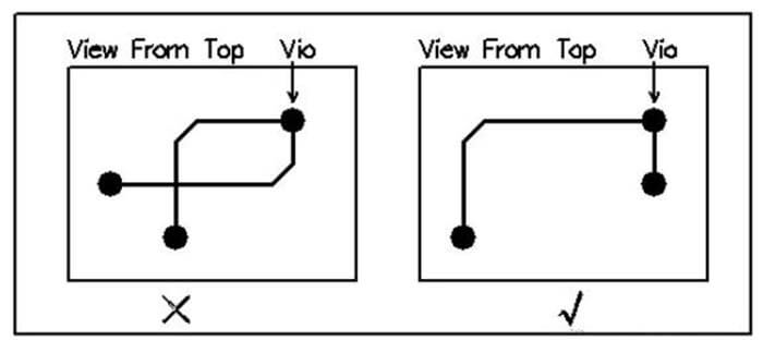
PCB design, pay attention to the formation of signal lines in different layers from the loop, especially in the multi-layer board wiring, the signal lines in the layers between the crosswalk, the formation of self-loop chances are greater, self-loop will cause radiation interference.
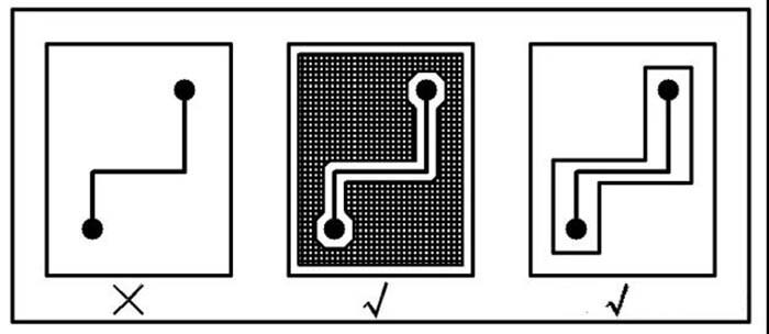
PCB design rule 3. The principle of minimum ground loop
Ground loop minimum rules, that is, the signal line and its loop to form the smallest possible ring area, the smaller the ring area, the less external radiation, and the less interference received from the outside world.
For this rule, in the ground plane division, to take into account the ground plane and the distribution of important signal lines, to prevent the problems caused by the ground plane slotting, etc.
In the double-layer board design, in the case of leaving enough space for the power supply, the part left should be filled with a reference ground, and add some necessary vias to effectively connect the two-sided signal, try to use ground isolation for some key signals, for some higher frequency design, special consideration needs to be given to its ground plane signal loop problem, it is recommended that the use of the multi-layer board is appropriate.
PCB design rule 4. High-speed signal shielding design
The corresponding ground loop rule, in fact, is also to minimize the signal loop area, mostly used for some of the more important signals, such as clock signals, synchronization signals.
For some particularly important, particularly high-frequency signal, should consider using copper shaft cable shielding structure design, that is, the line of the cloth up and down around the ground line isolation, but also consider how to effectively let the shield ground and the actual ground plane effectively combined.
PCB design rule 5. Avoid the "antenna effect"
Generally do not allow one end of the floating wiring, mainly to avoid the “antenna effect” to reduce unnecessary interference radiation and acceptance, otherwise, it may bring unpredictable results.
PCB design rule 6. Chamfering rules
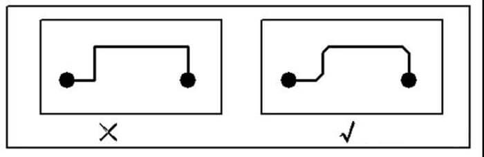
PCB design should be avoided to produce sharp angles and right angles, producing unnecessary radiation, while process performance is also bad. The angle of all lines and lines should be ≥ 135 °.
PCB design rule 7. Avoid overlapping different power supply layers
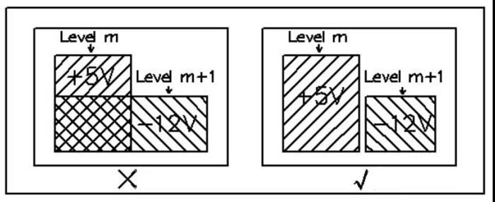
Different power supply layers in space to avoid overlap, mainly to reduce interference between different power supplies, especially between some power supplies with very different voltages, the problem of overlapping power supply planes must try to avoid, difficult to avoid when you can consider the interval ground layer.
PCB design rule 8. 3W rule
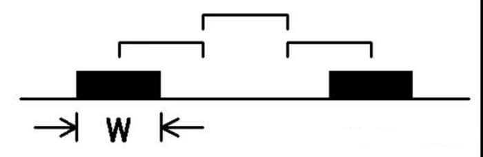
In order to reduce the line between the tampering, should ensure that the line spacing is large enough, when the line center distance of not less than 3 times the line width, it can maintain 70% of the electric field does not interfere with each other, known as the 3W rule. If you want to achieve 98% of the electric field does not interfere with each other, you can use the 10W rule.
PCB design rule 9. 20H rule
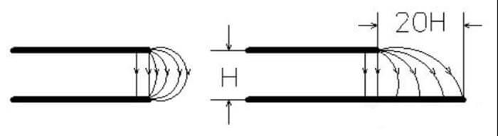
Since the electric field between the power layer and the ground layer is variable, electromagnetic interference will be radiated outward at the edge of the board. It is called the edge effect. The power supply layer can be inwardly shrunk so that the electric field is conducted only in the range of the grounding layer.
In terms of one H (thickness of dielectric between power and ground), if the inward shrinkage is 20H, 70% of the electric field can be confined within the ground edge; if the inward shrinkage is 100H, 98% of the electric field can be confined.
PCB design rule 10. Filter capacitor configuration rules (for reference only)
(1) The configuration of a high-frequency filter capacitor
Small-scale integrated circuit with less than 10 outputs, f ≤ 50MHz, and at least one 100nf filter capacitor. f ≥ 50MHz, each power pin with a 100nf filter capacitor.
For medium and large-scale integrated circuits, each power supply pin is connected with a 100nf filter capacitor. For circuits with large redundancy of power supply pins, the number of mating capacitors can also be calculated according to the number of output pins, with one 100nf filter capacitor for every five outputs.
For the area without active devices, at least one 100nf per 6 cm2 should be connected.
For UHF circuits, connect a 1nf filter capacitor to each power supply pin. For circuits with large redundancy of power supply pins, the number of capacitors can be calculated based on the number of output pins, with one 1nf filter capacitor for every five outputs.
For dedicated circuits refer to the recommended filter capacitor configuration in the application manual.
For circuits or areas with multiple power supplies, each power supply should be connected with filtering capacitors according to 1, 2, and 3 respectively.
The high-frequency filtering capacitor should be as close as possible to the power supply pins of the IC circuit.
Filter capacitor pads to the connection plate should be 0.3mm thick wire connection, the interconnection length should be ≤ 1.27mm.
(2) Configuration of low-frequency filter capacitors
Every 5 high-frequency filter capacitors should be connected with at least one 10μf low-frequency filter capacitor.
Every 5 10μf at least two 47μf low-frequency filter capacitors.
For every 100cm2, at least one 220μf or 470μf low-frequency filter capacitor should be connected.
Each module power outlet should be configured around at least two 220μf or 470μf capacitors, if space allows, the number of capacitors should be increased appropriately.
Low-frequency filter capacitors should be placed evenly around the filtered circuit.
PCB design rule 11. Select the correct grid
Set and always use the grid spacing that matches the largest number of components. Although multiple grids may seem to have significant utility, engineers who can think more in the early stages of PCB layout design will be able to avoid spacing setup problems and can maximize the application of the board.
As many devices are used in a variety of package sizes, engineers should use the most conducive to their own design products. In addition, polygons are critical for board coppering, multiple grid boards in polygonal coppering will generally produce polygon fill deviation, although not as standard as based on a single grid, but can provide more than the required board life.
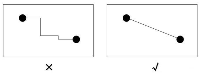
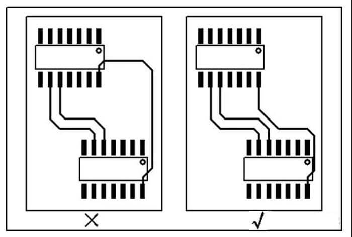
PCB design rule 12. Keep the path shortest and most direct
This may sound simple and unusual, but it should be kept in mind at every stage, even if it means changing the board layout to optimize the wiring length. This point also applies in particular to system performance is always partly limited by the impedance and parasitic effects of analog and high-speed digital circuits.
PCB design rule 13. Use the power supply layer as much as possible to manage the distribution of power and ground lines
Power layer copper for most PCB design software is a faster and simpler option. By connecting a large number of wires in common, you can ensure the highest efficiency and minimum impedance or voltage drop of the current, while providing sufficient ground return path.
If possible, you can also run multiple power supply lines in the same area of the board to confirm whether the ground layer covers most of the layers of a PCB, which facilitates the interaction between adjacent layers running lines.
PCB design rule 14. Group-related components together with the required test points
For example, the discrete components required for OpAmp op-amps are placed closer to the device so that the bypass capacitors and resistors can work with it on the same ground, thus helping to optimize the wiring length mentioned in the rule two, while also making testing and fault detection easier.
PCB design rule 15. Replicate the required board several times on another larger board for PCB layout
Select the most suitable size for the manufacturer’s equipment used to help reduce the cost of prototyping and manufacturing.
First, in the panel board layout, contact the board manufacturer to obtain their preferred size specifications for each panel, then modify your design specifications, and try to repeat your design within these panel sizes several times.
PCB design rule 16. Integrate component values
As a designer, you will choose discrete components that have either high or low component values, but the same performance. By integrating within a smaller range of standard values, you can simplify the bill of materials and potentially reduce costs.
If you have a range of PCB products based on preferred device values, it is also better for you to make the right inventory management decisions in the longer term.
PCB design rule 17. Perform as many design rule checks (DRC) as possible
Although it takes only a short time to run the DRC function on the PCB software, in more complex design environments, as long as you always perform checks during the design process can save a lot of time, it is a good habit to maintain.
Every wiring decision is critical, and by running DRC you can always be reminded of the most important ones.
PCB design rule 18. Use screen printing flexibly
Screen printing can be used to mark a variety of useful information for future use by board builders, service or test engineers, installers, or equipment commissioners.
Not only marked with clear function and test point labels but also as far as possible to mark the direction of components and connectors, even if these notes are printed on the lower surface of the components used on the board (after the board is assembled).
The full application of screen printing technology on the upper and lower surfaces of the board can reduce duplication of effort and streamline the production process.
PCB design rule 19. Must choose decoupling capacitors
Do not try to avoid decoupling power lines and optimize your design based on the limits in the component datasheet.
Capacitors are inexpensive and rugged, and you can spend as much time as possible assembling the capacitors while following rule number six, using a standard range of values to keep your inventory tidy.
PCB design rule 20. Generate PCB manufacturing parameters and verify them before submitting them for production
Although most board manufacturers are happy to download and verify them directly for you, it is best to export the Gerber file yourself and check that it is as expected with the free viewer to avoid misunderstandings.
By verifying it yourself, you may even find some inadvertent errors and thus avoid losses by completing production with the wrong parameters.
Besides the 20 Golden PCB Design Rules article, you may also be interested in the below articles.
PCB Antenna VS. External Antenna
Ceramic Antenna VS. PCB Antenna, A Comparison Guide
Wifi vs. 5G, is 5G better than Wifi?
Mobile Networks’ Evolution From 1G To 5G