Antenna Design
PCB Antenna Design
C&T RF Antennas Inc provides the PCB antenna design service and PCB antenna manufacturing along with the existing well-designed PCB antenna styles for your choice.
FPC Antenna Design
C&T RF Antennas Inc provides the FPC antenna design service and FPC antenna manufacturing along with the existing well-designed FPC antenna styles for your choice.
2.4GHz Antenna Design
This article talks about 2.4GHz antenna design, from theory to simulation to processing to testing.
This article introduces the design of the antenna is simple terms and recommends two tested low-cost PCB antennas. These PCB antennas can be used in conjunction with Bluetooth Low Energy (BLE) solutions.
We have A Complete Guide For PCB 2.4G Antenna Design for your reference also.
In order to achieve the best performance, the BLE 2.4 GHz radiofrequency must be correctly matched to its antenna. The last part of this application note describes how to debug the antenna in the final product.
Antenna Introduction
The antenna is a key component in the wireless system, it is responsible for sending and receiving electromagnetic radiation from the air.
Designing antennas for low-cost, consumer-wide applications and integrating them into handheld products is a challenge that most original equipment manufacturers (OEMs) are facing.
The wireless range that the end customer obtains from a certain RF product (such as a coin-type battery with limited power) mainly depends on the antenna design, plastic housing, and good PCB layout.
For systems with the same chip and power supply but the different layout and antenna design practices, it is normal for their RF (radio frequency) range to vary by more than 50%.
This application note introduces best practices, layout guidelines, antenna tuning procedures, and gives the widest band that can be obtained with a given amount of power.
A well-designed antenna can expand the working range of wireless products. The greater the energy sent from the wireless module, the greater the transmission distance under the conditions of the given packet error rate (PER) and the fixed receiver sensitivity.
In addition, antennas have other less obvious advantages. For example, a well-designed antenna can emit more energy within a given range, thereby improving error tolerance (caused by interference or noise).
Similarly, a good debugging antenna and Balun (balancer) at the receiving end can work under extremely small radiation conditions.
The best antenna can reduce PER and improve communication quality. The lower the PER, the fewer retransmissions will occur, which can save battery power.
Antenna Principle
Antennas generally refer to conductors that are exposed in space. When the length of the conductor is in a specific ratio or integer multiple of the signal wavelength, it can be used as an antenna. Because the power supplied to the antenna is radiated into the space, this condition is called resonance.
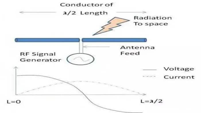
Figure 1. Basic dipole antenna
As shown in Figure 1, the wavelength of the conductor is λ/2, where λ is the wavelength of the electrical signal. The signal generator is powered by a transmission line (also called antenna feed) at the center of the antenna. According to this length, a standing wave of voltage and current will be formed on the entire wire, as shown in Figure 1.
The electrical energy input to the antenna is converted into electromagnetic radiation and radiated into the air at the corresponding frequency. The antenna is fed by the antenna with a characteristic impedance of 50Ω and radiates into space with a characteristic impedance of 377Ω.
Therefore, regarding the geometry of the antenna, there are two very important things to note:
1. Antenna length
2. Antenna feed
An antenna with a length of λ/2 (as shown in Figure 1) is called a dipole antenna. However, in printed circuit boards, most of the conductors used as antennas are only λ/4 in length, but they still have the same performance. See Figure 2.
By placing a ground plane at a certain distance below the conductor, a mirror image (λ/4) of the same length as the conductor can be created. When combined, these pins act as dipole antennas.
This type of antenna is called a quarter-wavelength (λ/4) antenna. Almost all antennas on the PCB are implemented in the size of a quarter-wavelength on the copper ground plane. Note that the signal is now a single-ended feed, and the ground plane is used as the return path.
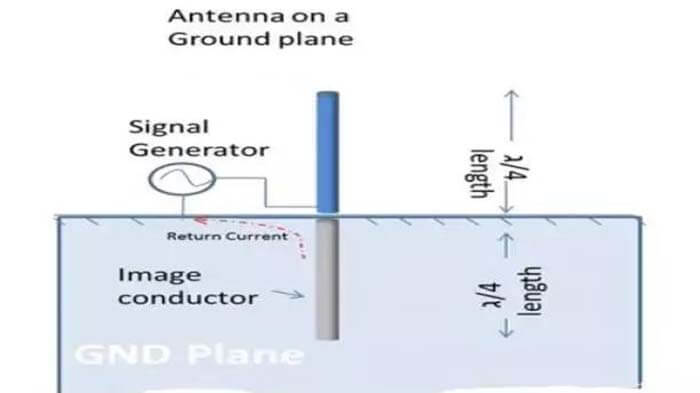
Figure 2. Quarter-wavelength antenna
For the quarter-wave antennas used in most PCBs, special attention is needed:
1. Antenna length
2. Antenna feed
3. The shape and size of the ground plane and return path
Antenna Types
As mentioned in the previous section, all conductors with a wavelength of λ/4 exposed in free space are placed on a ground plane and provided with a suitable voltage, then the conductor can be used as an antenna.
Depending on the wavelength, the antenna may be as long as the FM antenna of a car, or as short as the trace on the signal buoy. For 2.4GHz applications, most PCB antennas belong to the following types:
Antenna type 1. Wire antenna
This is a section of wire extending into the free space on the PCB, its length is λ/4, and it is placed on the ground plane. This antenna is powered by a 50Ω impedance transmission line.
Generally, the wire antenna provides the best performance and radiation range. The wire can be straight, spiral, or looped. It is a three-dimensional (3D) structure in which the antenna is 4-5mm higher than the PCB and extends into space.
Antenna type 2. PCB antenna
It is a PCB trace on the PCB, and it can be drawn as a straight trace, an inverted F-shaped trace, a serpentine or circular trace, etc.
In a PCB antenna, unlike the wire antenna, the antenna is not exposed to the external space, but exists in a two-dimensional (2D) structure on the same PCB layer; see Figure 3.
When the 3D antenna exposed to space is placed on the PCB layer as a 2D PCB trace, certain guidelines must be followed.
Under normal circumstances, compared with wire antennas, it requires more PCB space, low efficiency, but low cost, and can provide BLE applications with a receivable wireless distance.
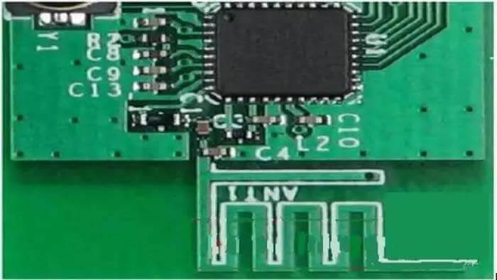
Figure 3. PCB antenna
Antenna type 3. Chip antenna
This is an antenna with a conductor. Both the antenna and the conductor are assembled in a small IC package. When the antenna is packaged in a small size, it becomes very advantageous.
Applications such as antenna USB nano transceivers will use this antenna when there is not enough space on the PCB to layout the PCB antenna.
Antenna Selection
The selection of antenna depends on factors such as its application, available circuit board size, cost, radiation range, and directivity.
Bluetooth Low Energy (BLE) applications (such as a wireless mouse) only require a 10-inch radiation range and a data rate of a few kbps.
However, for remote control applications using voice recognition, an indoor antenna is required. The antenna’s radiation range is about 10-15 inches, and its data rate is 64kbps.
For wireless audio applications, a diversity antenna is required.
Diversity antenna means that two antennas are placed on the same PCB. This ensures that at least one antenna can always receive some radiation, while the other antenna may be blocked due to reflection and multipath attenuation.
In the case of transmitting real-time audio data and requiring higher throughput without losing data packets, a diversity antenna is required. It can also be used in beacon applications for indoor positioning.
Antenna Parameters
The following section provides some key parameters of antenna performance.
Return loss
The return loss of the antenna indicates how the antenna is matched to a transmission line (TL) with an impedance of 50Ω, which is shown as the signal feed-in Figure 4.
Usually, the impedance value of this TL is 50Ω, but other values are also possible. For industry standards, the resistance of a commercial antenna and its test equipment is 50Ω, so it is recommended that you use this value.
The return loss indicates the amount of incident power reflected by the antenna due to the mismatch (Equation 1). An ideal antenna will emit all the power without any reflections.
Formula 1 Return Loss (dB) = 10 log (Pincident/Preflect)
If the return loss is infinite, it is considered that the antenna matches the TL completely, as shown in Figure 4. S11 is the reciprocal of the return loss, and its unit is dB. According to empirical estimates, if the return loss is greater than or equal to 10dB (that is, S11≤-10dB), it will be large enough.
Table 1 shows the return loss (dB) and reflected power (%) of the antenna. When the return loss is 10dB, it means that 90% of the incident power is transmitted to the antenna for transmission.
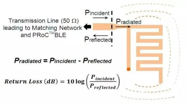
Figure 4. Return loss
| S11 | Return Loss | Preflected/Pincident | Preflected/Pincident |
| (dB) | (dB) | (%) | (%) |
| -20 | 30 | 1 | 99 |
| -10 | 10 | 10 | 90 |
| -3 | 3 | 50 | 50 |
| -1 | 1 | 79 | 21 |
Table 1. Antenna’s return loss and reflected power
Bandwidth
Bandwidth refers to the frequency response of the antenna. It shows how the antenna and the 50Ω transmission line match each other in the entire frequency band used, that is, in the range of 2.40GHz to 2.48GHz for BLE applications.
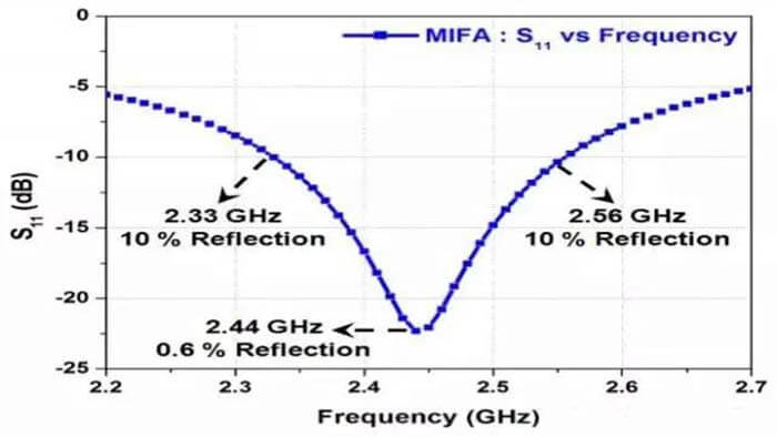
Figure 5. Bandwidth
As shown in Figure 5, in the 2.33GHz to 2.55GHz bandwidth, the return loss is greater than 10dB. Therefore, the bandwidth used is about 200MHz.
Radiation efficiency
Radiation efficiency means that part of the non-reflective power consumption is consumed as heat in the antenna.
The heat generated is due to the dielectric loss in the FR4 substrate and the conductor loss in the copper wire. This information serves as radiation efficiency.
When the radiation efficiency is 100%, all non-reflective power consumption is emitted into space. For small PCB form factors, the heat loss is minimal.
Radiation pattern
The antenna radiation pattern represents the directivity of radiation, that is, in which direction the radiation is greater and which direction the radiation is smaller. This helps to accurately determine the direction of the antenna in the application.
The non-directional antenna can transmit equivalently in all directions on a plane perpendicular to the axis. But most antennas cannot achieve this ideal performance.
Each data point represents the RF field strength, which can be measured by the Received Signal Strength Indicator (RSSI) in the receiver. As expected, the contour image obtained is not circular because the antenna is not isotropic.
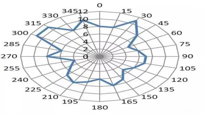
Figure 6. Radiation pattern
Antenna gain
The antenna gain provides information for comparing the radiation of the used direction with an isotropic antenna (that is, transmitting from all directions).
The gain unit is dBi, which means the radiated field strength when compared with an ideal non-directional antenna.
C&T RF Antennas Inc’s antenna design
One of the limiting factors in the design of a BLE PCB antenna is the need to integrate the antenna in a compact space, and only two external components can be used for adjustment.
The debugging process needs to ensure that the energy of the incoming antenna should be maintained as much as possible when transmitting in a certain frequency band. This means that the return loss in the required band should be greater than 10dB.
When the input impedance of the antenna is 50Ω and the output impedance of the chip is 50Ω, the energy received by the antenna is the largest. When the antenna is used as the receiving end, the above conditions must also be met.
For the antenna, its adjustment process can ensure that the impedance of the antenna is equal to 50Ω. For the chip, the Balun (balancer) adjustment process can ensure that the resistance is close to 50Ω.
The PCB antenna recommended by C&T RF does not require any components to adjust the antenna.
In addition, C&T RF Antennas Inc also provides antenna designs for different applications, such as indoor positioning antenna design, smart home antenna design, smart appliance antenna design, and sensor antenna design.
Antenna designs for these applications may not be limited by space. Therefore, better antennas can be designed for these applications according to factors such as radiofrequency range and radiofrequency pattern. Wire antennas are very suitable for non-wearable but fixed location applications.
Many applications directly embed the antenna design of C&T RF Antennas Inc in their main PCB for wireless connection.
Although there are many applications that use the 2.4GHz frequency band, most BLE applications only use the two PCB antennas described below. C&T RF Antennas Inc recommends the use of two proprietary PCB antennas, the serpentine inverted F antenna (MIFA) and the inverted F antenna (IFA), which are characterized and extensively simulated antennas for BLE applications. Especially MIFA, it can be used in almost all Bluetooth/Wifi applications.
PCB antenna designed by C&T RF Antennas Inc
PCB antennas are widely used in single-band module circuit boards such as Bluetooth modules, WIFI modules, and ZIGBEE modules.
Advantages:
The cost is very low, and there is no need to debug again after one debugging.
Disadvantages:
Suitable for a single frequency band, such as Bluetooth, WiFi.
The performance of PCB antennas of different batches will have certain deviations.
C&T RF Antennas Inc recommends the use of IFA and MIFA PCB antennas. The low rate and typical radiation range in BLE applications make these two antennas particularly useful.
These antennas are cheap and easy to design because they are an integral part of the PCB and can provide good performance in the 150 to 250 MHz frequency range.
It is recommended to use MIFA antennas in applications that require only minimal PCB space, such as wireless routers, keyboards, demonstration machines, and so on.
For the IFA antenna, it is recommended to apply it to applications that require the size of one side of the antenna to be much smaller than the size of the other side, such as a heart rate monitor. MIFA antennas are used in most BLE applications. The following sections will detail the information of each antenna.
Serpentine inverted F antenna (MIFA)
MIFA is a common antenna that is widely used in various human interface devices (HID) because it occupies a small PCB space.
Therefore, C&T RF Antennas Inc has designed a robust MIFA antenna that can provide superior performance in a smaller form factor. It is very suitable for various HID applications, such as wireless routers, keyboards, or demo machines.
Figure 7 shows the detailed layout of the recommended MIFA antenna, which includes the top and bottom layers of a double-layer PCB. The value of W is the main parameter that can be changed. It depends on the PCB stacking interval. It represents the width of the RF trace (transmission line).
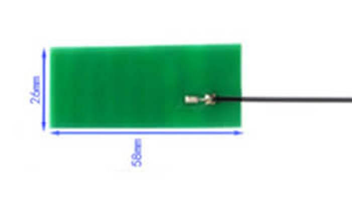
Figure 7. MIFA layout PCB antenna
For PCB traces that feed shorter antennas, such width requirements are relatively loose. Make sure that the width of the antenna trace is the same as the width of the antenna feed contact.
The consideration of antenna length According to the different thicknesses of the PCB, the length of the MIFA antenna needs to be adjusted so that the impedance and frequency selection of the antenna radiation can be adjusted.
Inverted F antenna (IFA)
For applications that have certain restrictions on the size of the antenna but require a good antenna design, it is recommended that you choose this IFA. Figure 8 shows the recommended IFA antenna.
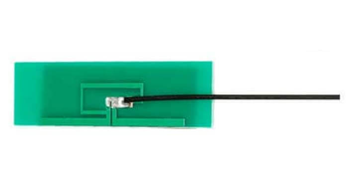
Figure 8. IFA inverted F antenna
Flex PCB / FPC antenna designed by C&T RF Antennas Inc
Cellular/WiFi multi-band embedded flexible PCB antenna
The FPC antenna is equivalent to pulling out the antenna line on the PCB board and using other external metal as the antenna. Usually used in low-end mobile phones and smart hardware products with complex frequency bands.
Advantages:
It is suitable for almost all small electronic products and can be used as a complex antenna with more than ten frequency bands, with good performance and relatively low cost.
Disadvantages:
It needs to be debugged separately according to each product.
LDS antenna designed by C&T RF Antennas Inc
The LDS antenna is an evolved version of the FPC antenna, with extremely high space utilization. The FPC line is stamped out, and it must be flat, and complex shapes cannot be stamped out.
The FPC antenna is a whole plane, although it can be bent, it can’t be made too complicated. LDS antennas use lasers to engrave the antenna’s graphics, which is very suitable for applications with compact internal space.
Advantages:
It can make full use of various irregular surfaces in the three-dimensional space and reduce the size of the antenna.
Disadvantages:
The price is more expensive, an order of magnitude more expensive than the FPC antenna, and there are many special requirements for the process of the outer surface of the product.
The influence of environment on antenna performance
Generally, antennas used in consumer products are very sensitive to the size of the PCB radio frequency ground layer and the product’s plastic casing.
The antenna can be simulated as an LC resonator. When L (inductance) or C (capacitance) increases, the resonance frequency of the LC resonator will decrease. A larger RF ground plane and plastic housing will increase the effective capacitance, thereby reducing the resonant frequency.
The influence of the ground plane
To evaluate the sensitivity of the antenna to the size of the RF ground plane, experiments can be carried out by installing the antenna on PCBs of various possible sizes.
Figure 9 shows an example of MIFA placed on a PCB with different ground plane sizes. The size of PCB ranges from 20mm×20mm to 50mm×50mm.
It can be understood from this curve that the larger the area of the RF grounding layer, the lower the resonance frequency and the better the grounding layer, so the return loss will be smaller.
This is the key condition in a good PCB layout. The better the ground plane provided for the quarter-wavelength antenna, the better the relationship between it and the theoretical performance.
This is a key concept in antenna design, which can solve the difficulty of not having enough space for grounded small modular antennas.
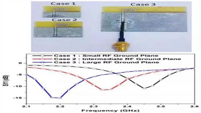
Figure 9. PCB Antennas
Product housing and ground plane guide
- It must be ensured that there are no components, fixing screws or ground planes near the tip of the antenna or the length of the antenna.
- The battery cable or audio cable cannot pass through the same side of the antenna or the antenna wiring on the PCB.
- Do not completely cover the antenna with the metal case. If the product shell is metal or a protective cover, please do not completely cover the antenna.
- The direction of the antenna should match the direction of the final product so that the antenna has the maximum radiation in the desired direction.
- There should be enough space: the larger the ground layer, the higher the S11 parameter value (return loss) of MIFA, IFA, chip antenna, and wire antenna.
- There should not be any ground plane directly below the antenna. This setting applies to all antennas.
- There must be enough space (gap) from the antenna to the ground plane, and the width of the ground plane should be the smallest.
Antenna debugging
Antenna debugging is an important part of antenna design.
The antenna debugging process ensures that the return loss of the antenna (viewed from the direction of the chip output) is greater than 10dB in the required frequency band.
Similarly, for the chip (Balun), the same procedure must be performed to ensure that the impedance of the Balun is 50Ω in the receiving mode. At this time, both antenna debugging and Balun debugging are called antenna debugging.
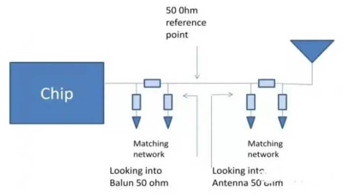
Figure 10. Reference diagram of debugging and matching network
The 50Ω reference point is connected to a network analyzer with a port network. During antenna debugging, the connection with the chip can be disconnected by removing the Balun matching component. During Balun debugging, the connection with the antenna matching component will be disconnected.
Debugging process
As mentioned earlier, the influence of the housing and the ground plane detunes the required frequency band of the antenna and affects the return loss. Therefore, the antenna debugging process includes two steps.
First, debug the empty PCB board to the required frequency band; then after determining the ID, check and debug through the contact of the plastic casing with the human body.
Use a network analyzer to check the antenna debugging. In the first step, the network analyzer is calibrated first, and then the antenna debugging is performed by adjusting the matching network components and verifying the debugging in the Smith chart.
Summarize
This article briefly introduces how to customize the best antenna design for the product. At the same time, it also provides antenna layout guidelines for different antenna design types.
C&T RF Antennas Inc provides the existing PCB antenna designed products, FPC antenna designed products, spring antenna designed products, rubber duck antenna designed products, fiberglass antenna designed products, magnetic mount antenna designed products, through-hole screw mount antenna designed products, and other existing antenna designed products.
Contact us for more antenna designs and well-designed antenna products.