After the read of this Ceramic Antenna VS. PCB Antenna, A Comparison Guide article, you will learn:
Ceramic Antenna VS. PCB Antenna’s Definition
Ceramic Antenna VS. PCB Antenna’s Working Principle
Ceramic Antenna VS. PCB Antenna’s Category
Ceramic Antenna VS. PCB Antenna’s Performance Parameters
Ceramic Antenna VS. PCB Antenna’s Advantages
Ceramic Antenna VS. PCB Antenna’s Disadvantages
Ceramic Antenna VS. PCB Antenna’s Applications
Ceramic Antenna VS. PCB Antenna’s Design
Here we go!
Navigation antennas are more and more widely used in our life, such as cell phones, electronic watches, cars, navigation devices, and so on.
For different applications, navigation antennas are also divided into many kinds, such as internal antennas, GPS antennas, external antennas, timing antennas, etc. So what is the difference between the common ceramic antenna and the PCB antenna?
Ceramic Antenna VS. PCB Antenna’s Definition
What is a ceramic antenna?
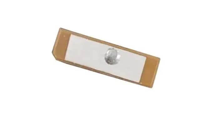
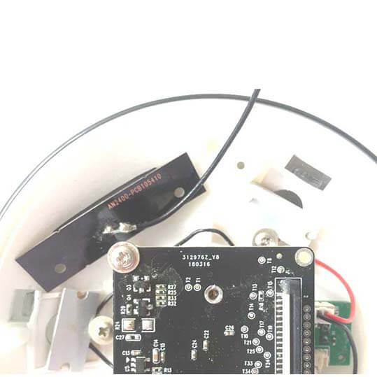
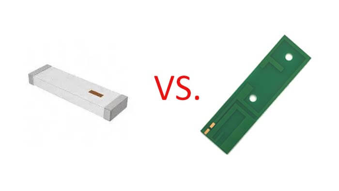
The ceramic antenna is a kind of miniaturized antenna suitable for Bluetooth devices, and it is divided into block ceramic antenna and multi-layer ceramic antenna.
The ceramic antenna is made of ceramic, which has a frequency range of 300MHz to 300GHz, and in terms of dielectric loss, the ceramic dielectric is less than the dielectric loss of the PCB board, so it is ideal for use in Bluetooth modules with low power consumption rates. The ceramic antenna is stronger than the on-board antenna, and generally has ANT access foot and ground foot, which is also very easy to use.
In addition, when using a ceramic antenna, also pay attention to the matching problem of the Babylon circuit, if it is with a special integrated circuit, it is best to let the manufacturer test the matching of the balancing circuit and ceramic antenna, if the matching is not good, it will also affect the effect of ceramic antenna.
What is a PCB antenna?
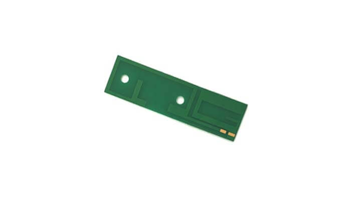
PCB antenna is the part on PCB for wireless receiving and transmitting. The antenna is a transducer.
When transmitting, it converts the high-frequency current from the transmitter into space electromagnetic waves.
When receiving, it converts the electromagnetic wave intercepted from space into a high-frequency current to send to the receiver.
For designing a small power, short-distance wireless transceiver applied in an RF identification system, antenna design is an important part of it.
A good antenna system can make the communication distance reach the best state. There are many kinds of antennas, and different applications need different antennas. In low-power, short-distance RFID systems, a reliable and inexpensive antenna system for communication is needed, PCB antenna is one of the more common ones.
Ceramic Antenna VS. PCB Antenna’s Working Principle
What is the working principle of ceramic antennas?
The principle of ceramic antenna should be divided into two parts: one is the transmitting antenna, and one is the receiving antenna.
Ceramic antenna transmitting antenna simply put, is through a called antenna electrode between the antenna and the formation of the high-frequency electric field into electromagnetic waves, so as to be able to transmit out and wave to the far side.
Ceramic antenna receiving antenna simply put is through an electrode called the antenna will be the air from the electromagnetic wave induction into the electric field, generate high-frequency signal voltage, and sent to the receiver for signal processing.
What is the working principle of PCB antennas?
The PCB antenna receives electromagnetic waves and converts them into electrical signals, or receives electrical signals and radiates them as electromagnetic waves.
Ceramic Antenna VS. PCB Antenna’s Category
Ceramic antenna categories
Block antenna
Block antenna uses high temperature to sinter the whole ceramic body once and then print the metal part of the antenna on the surface of the ceramic block.
Multi-layer antenna
Multi-layer antenna sintering uses a low-temperature co-firing method to iterate and align the multi-layer ceramic and then sinter it at high temperature, so the metal conductor of the antenna can be printed on each layer of ceramic media layer according to the design needs, so it can effectively reduce the size of the antenna and can achieve the purpose of hiding the antenna.
Because the ceramic itself has a higher dielectric constant than the PCB board, the use of a ceramic antenna can effectively reduce the size of the antenna under the condition of ensuring the antenna performance.
PCB antenna structure categories
PCB antenna structure can be monopole, dipole, slot, patch, and planar inverted F (PIFA).
Dipole and monopole PCB antenna
The dipole antenna consists of two-quarter wavelength (λ/4) long metal strips with a total electrical length required to be half wavelength (λ/2) below the carrier frequency to achieve maximum response. Due to the widespread use of legacy protocols such as Bluetooth and Wi-Fi, much of the antenna literature focuses on antenna design in the 2.4 GHz ISM band.
Bending monopole antenna
The bent monopole variants of L-shaped (or tilted whip and inverted L), planar inverted F (PIFA) and zigzag inverted F (MIFA) structures utilize the same grounding element and conductive arm approach, but with different conductive arm patterns. The bending of the alignment allows for more compact dimensions as well as a reduction in the zero point in the radiation direction diagram.
However, in these designs, the antenna alignment usually cannot be too close to the ground, which would cause the antenna to act as a transmission line without any radiation.
PIFA is the most common among these variants because of its smaller PCB area and wide bandwidth performance.
In MIFA, the horizontal and vertical lines form multiple turns. As with PIFA, tuning is accomplished by adjusting the geometry within the zigzag lines. This effectively reduces the size of the antenna.
Dipole antenna variants
Printed dipole antennas mainly face a size disadvantage. This is particularly relevant for low frequencies; here, the advantage of a monopole antenna element is that it can be potentially placed in a corner of the board where the ground element is used both as the RF ground plane/return path for the antenna and as a ground element for the local electrical components of the crop networking module.
Ceramic Antenna VS. PCB Antenna’s Common Frequency Bands
What are the ceramic antenna frequency bands?
Ceramic antenna frequency bands are 2.4 GHz, 5 GHz, 2.4/5 GHz, LoRa, GPS, GSM, etc
What are the common frequency bands of PCB antennas?
2.4 GHz, 5 GHz, 2.4/5 GHz, GPS, GSM, NB-IoT, 2G 3G, 4G LTE 5G NR, Sub-6G, LoRa 315 MHz, 433 MHz, 868 MHz, 915 MHz, etc.
Ceramic Antenna VS. PCB Antenna’s Performance Parameters
What are the parameters that affect ceramic antennas?
The ceramic antenna has four important parameters: Gain, VSWR, Noise figure, and Axial ratio. Especially emphasize the Axial ratio, which is an important index to measure the difference in signal gain of the whole machine in different directions.
What are the factors that affect the performance parameters of PCB?
Flatness
According to the characteristics of the PCB and the production process, we know that it is bonded and crimped layer by layer, the manufacturing process will have stress, and the pad layer and the middle of the material, and the thickness of the electrical isolation layer is different, so the coefficient of thermal expansion is also different, and thus in the packaging and transportation process, the PCB may be bow or twist, the degree of plastic deformation The thickness and area of the PCB and its board design is symmetrical and other related.
PCB bending, twisting the allowable value of the PCB length L 0.75%, that is, (L × 0.75%) mm, but the maximum can not exceed 3.175 mm.
If the flatness exceeds the allowable range, the shape of the datum in the camera will change, for example, the shape of the standard circular datum in the camera will become elliptical, which will lead to changes in the center distance reading between the datum, which will affect the position of the component pads on the PCB relative to the datum, and thus may directly cause the component paste bias.
In addition, the placement process in the PCB warpage will lead to components in the process of downward pressure relative to the solder paste on the pad sliding, or the bottom of the component solder paste squeezed away, thus forming a tin bead or lead to adjacent components bridging short circuit.
The influence of manufacturing tolerance
PCB manufacturing tolerance will also have an influence on the placement quality, mainly in the reference point (Fiducial) contour degree and position degree deviation, as for PCB other errors, such as over-hole manufacturing tolerance will directly affect soldering after the electrical performance, but this does not belong to the impact on the bonder.
Surface treatment
The surface treatment for the placement influence, mainly embodies the reference point (Fiducial) the coverage aspect, can mainly influence the visual image system can accurately, and quickly identifies the reference point. The important principle is, the solder resist layer can not cover the reference point and its surrounding auxiliary resolution area.
Ceramic Antenna VS. PCB Antenna’s Advantages
Advantages of ceramic antenna
Ceramic antenna occupies little space and has better performance.
Narrow bandwidth, more difficult to do multi-band.
Effectively improve the integration of the motherboard and can reduce the limitation of the antenna to the ID. Need to import the design at the beginning of the definition of the motherboard.
PCB antenna advantages
PCB can be more and more widely used, because it has many unique advantages, as follows.
PCB antenna advantages are less space occupation, low cost, no need to assemble the antenna separately, not easy to touch damage, and ease to assemble the whole machine.
Can be high density
For decades, the printed board’s high density can be developed with the integrated circuit integration increase and installation technology progress.
High reliability
A series of inspections, testing, and aging tests can ensure that the PCB long-term (use period, generally 20 years) and reliable work.
Designability
Various performance (electrical, physical, chemical, mechanical, etc.) requirements of PCB can be standardized and standardized by design to achieve printed board design, short time, and high efficiency.
Producibility
With modern management, standardization, scale (quantity), automation, and other production can be carried out to ensure consistent product quality.
Ceramic Antenna VS. PCB Antenna’s Disadvantages
The disadvantage of the ceramic antenna is that it is difficult to do multi-band, so it is difficult to be used in 4G products. Higher board headroom requirements are not suitable for particularly compact products.
The disadvantage of PCB antenna is that it is difficult to round the individual antenna field shape, has high insertion loss, relatively low efficiency, and is easy to interfere with the motherboard.
- PCB antenna performance is worse than FPC antenna and other types.
- The material of PCB after mass production, batch, if the replacement board factory will seriously affect the performance of the antenna.
- The frequency band range is generally narrower.
- Because the antenna and PCB height does not form a height difference, the design of the structure is also very limited.
Ceramic Antenna VS. PCB Antenna’s Applications
What are the applications of ceramic antennas?
The ceramic antenna is widely used in Bluetooth headsets, smartwatches, Bluetooth electronic cigarettes, smart small home appliances, smart medical, smart home products, etc.
What are the applications of PCB antennas?
PCB antennas are widely used in Bluetooth modules, WIFI modules, ZIGBEE modules, GPS modules, 4G modules, NB-IoT modules, and other frequency band module circuit boards.
Ceramic Antenna VS. PCB Antenna’s Design
How to design a ceramic antenna?
The ceramic antenna design used high frequency, low noise amplifier, in order to attenuate the antenna thermal noise and the front several levels of the unit circuit on the receiver performance, and the role of the ceramic antenna is to transform the electromagnetic wave energy of the radio signal from the satellite into the receiver electronics can take in the application of current, so the size and shape of the antenna are very important.
How to design a PCB antenna?
2.4 GHz PCB antenna, if you do not consider the cost and size, you can choose other antennas, such as patch antenna (small size, medium performance, medium cost) or external whip antenna (large size, high performance, high cost), and PCB antenna is the lowest cost, medium size, as long as the design is right and can get enough performance antenna.
Three types of antennas are included: ultra-small PIFA antenna, normal PIFA antenna, normal Wiggle antenna.
PCB antenna design considerations
(1) The PCB board below the antenna needs to be clear, with no copper cladding, and no metal devices placed near the antenna.
(2) RF alignment around the need to lay copper, including the bottom layer, copper laying in accordance with the impedance requirements for implementation, and the best solid copper laying.
(3) RF alignment around more irregular GND over the hole.
(4) antenna matching device requirements and RF alignment on the same road.
(5) RF alignment in strict accordance with 50 ohms to do, and RF can be short on short.
Can ceramic antenna or PCB antenna be used for 2.4 GHz and other high-frequency products?
Although 2.4 GHz and other high band products can use ceramic or PCB antennas to reduce the size, Sub-G requires larger size space to achieve the same gain due to the long electromagnetic wave wavelength, so the band products rarely use the above two antennas.
Besides the Ceramic Antenna VS. PCB Antenna, A Comparison Guide article, you may also be interested in the below articles.
Wifi vs. 5G, is 5G better than Wifi?
Mobile Networks’ Evolution From 1G To 5G
How To Choose Embedded Antenna For IoT?