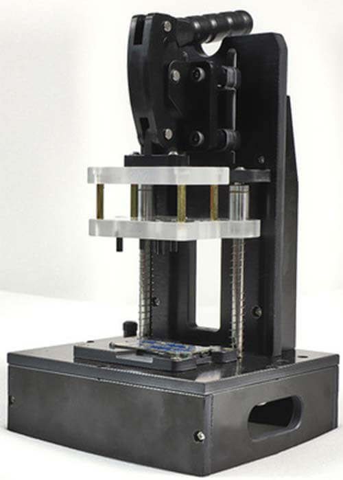
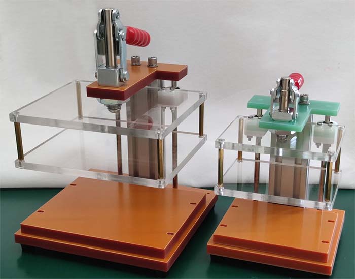
What is a PCB testing jig?
PCB testing jig can be identified as a PCB testing equipment, or PCB testing machine, it is a PCBA test fixture or test jig that is the component containing the bed of nails used for testing the PCB or assembled product.
What is the principle of a PCB testing jig?
The principle of the PCB testing jig is very simple, PCB test jig fixture is connected to the pads or test points on the PCB board through metal probes, under the condition of PCB board power, to obtain the voltage value, current value, and other typical values of the test circuit, so as to observe whether the circuit under test is conductive and normal.
PCB test jig fixture can be customized, and PCB test fixture can be designed, according to the size of the PCB board to be tested, the location of the test point, and the value to be tested to decide. Mainly using acrylic, plastic, metal probes, displays, and wires, and equipped with a simple PCB board to complete the entire production.
What is a PCB testing jig used for?
PCB testing jig is widely used in the whole PCB processing and production process, mainly used to test the PCB circuit board after the completion of SMT placement and DIP plug-in, which is mainly an ICT test, that is, through the test points to test the electrical conductivity of the circuit board, so as to determine whether the whole PCB board welding success. The PCB test jig fixture is the main tool used to assist in completing this test.
The quality of the PCB test stand is related to the efficiency of ICT testing and throughput rate, due to its long-term frequent operation, and the production quality of its high requirements, PCB manufacturers need to pay sufficient attention to it.
What is the main test of PCB test fixture?
PCB test jig fixture is used in the through test machine (ET-TEST) on the test jig, mainly used to test the lines on the circuit board, will not open and short circuit, to ensure the quality of PCB boards!
- To test whether there is a short circuit between different network alignments of the PCB.
- To test the PCB with the same network to each pad whether the open circuit, over the hole whether the open circuit.
- PCB board insulation strength test.
- PCB board impedance test.
How to make a PCB testing jig?
PCB test jig fixture is a kind of equipment used to test the finished PCB. In the PCB test jig design production, PCB fabricators usually need to provide Gerber files and PCB samples to facilitate the production of test jigs.
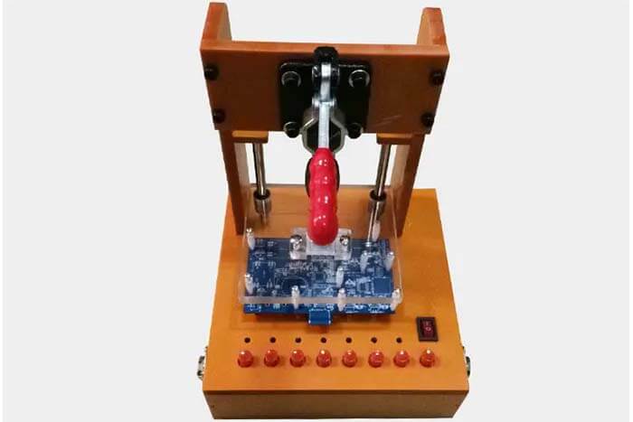
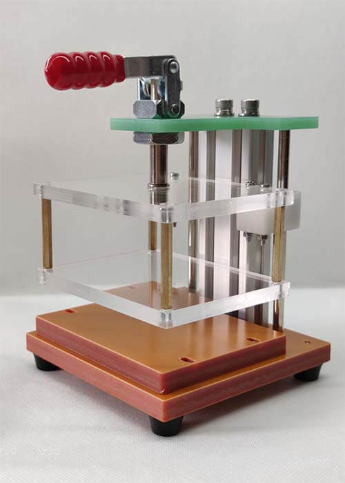
For the current stage of the PCB testing jig, only a few pressure plate buckles are installed on the PCB test fixture, and the PCB is fixed by the thimble and pressure plate buckles. During the PCB function test, the PCB is pressed into the platen buckle with both hands.
PCB due to uneven force or insufficient pressure, it is easy to make poor contact between the test pin and PCB, which seriously affects the efficiency and accuracy of the test; if the force is too much, the PCB is easily deformed or damaged when pressed down, it is also easy to damage the test pin of the test stand, causing greater losses.
PCB testing jig production steps
First, material preparation According to the information to determine the program, you need to prepare the hardware materials (electronic components), related additional peripheral circuits, equipment, frame materials (such as an acrylic board), glue, electrical batches, screws, wire materials, etc., to produce the program to determine the information.
Second, the test frame structure way to determine and check.
What is the PCB test jig design process?
- User requirements
Provide requirement description, PCB file, and front and back side physical photos to the C&T RF sales team
- Determine the solution and quotation
According to the customer’s requirements, and the discussion results to make accurate quotation and delivery time
- Engineering design
According to the technical parameters discussed earlier for detailed design, drawing
- Assembly and commissioning
Assemble and debug the parts processed by the production line
- Packaging and delivery
The assembled and debugged products are tested by QC and packaged for shipment
- After-sales maintenance
The shipped products have the operation or consumable accessories Follow-up maintenance
Note: Usually you need to provide 4 kinds of information:
- PCB drawing file_(CAD, GERBER, STP format can be opened), if there is no drawing file, then you need to provide an empty PSB for copy number.
- PCB photos with parts, front, side, and bottom, marked with higher DIP parts height.
- Please use the drawing tool to mark the lower pin position on the picture.
- Provide the physical board to facilitate the design and production process to adjust the PCB test jig fixture as normal.
If you have other production requirements, such as the PCB test jig fixture to be placed on the power switch, or socket.
If you have other production requirements, such as a power switch, socket, display screen, test board, etc., the customer’s samples need to provide the physical or dimensional drawings of the accessories, and the current and voltage meter need to indicate the specific range!
Why must the PCB test fixture be made of Bakelite material?
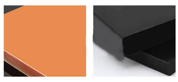
Bakelite is a thermosetting plastic, heat-resistant, not easy to age and becomes brittle; has high mechanical strength, good insulation properties, and corrosion resistance, especially suitable for electrical-related products, which is incomparable with any other materials.
Bakelite material is divided into A grade and B grade, the price difference between the two is not much, but the characteristics of the two materials are completely different, and the scope of application is completely different.
The PCB test jig fixture bakelite must be made of A-grade material. If you use B-grade material, the cost is not much different from A-grade, but the processing scrap rate of B-grade material will be many times higher than that of A-grade, so experienced manufacturers will not use B-grade material to do the test frame.
What are the PCB wiring requirements?
- Open wire opening needs to be opened within 2mm, the first wire opening tin and test pin tin wire bit tin.
- Solder the wire can not have swing and loosen phenomenon.
- The PCB testing jigs and fixtures in the strong and weak wires are separated and organized and wire-tied wire.
- Ammeter and voltmeter connectors must be selected for multimeter pen installation, cannot be installed banana plug test current and voltage and other functions to ensure the safety of the operator.
- High-frequency product models connected to the signal line must use shielding wire to ensure the safety of the external network grounding.
- The PCB testing jig with fire cattle must be grounded to the fire cattle shell.
- The PCB testing jig should be installed fuse, that cannot be replaced by wire or other wires, the original plug of the 13A fuse removal to remove, replace the fuse to pay attention to the test model needs how much current, the replacement principle by the product working current 8-10 times can be.
Contact C&T RF Antennas Inc for the PCB testing jigs PCB test jig design, or PCB test fixture components such as PCB test jig pins, PCB test fixture Bakelite board, etc.
Besides the What Is a PCB Testing Jig and How To Make It article, you may also be interested in the below articles.
Wifi vs. 5G, is 5G better than Wifi?
Mobile Networks’ Evolution From 1G To 5G
How To Choose Embedded Antenna For IoT?