When faced with a PCB design, there are 5 important attributes to consider when performing EMC PCB design guidelines analysis of a PCB product and design, the 5 EMC PCB Design Guidelines are as follows.
1. Critical device size for EMC PCB design guidelines
The physical size of the emitting device that generates the radiation. The length of the PCB alignment has a direct impact on the RF current as a transmission path.
2. Impedance matching of the EMC PCB design guidelines
Impedance matching source and receiver impedance, and the transmission impedance between the two.
3. EMC PCB design guidelines of the temporal characteristics of the interference signal
Whether the problem is a continuous (periodic signal) event or only exists in a specific operation cycle (for example, a single event may be a certain keystroke operation or power-up disturbance, periodic disk drive operation, or network burst transmission).
4. The strength of the interference signal for EMC PCB design
How strong the source energy level is, and how much potential it has to generate harmful interference.
5. Frequency characteristics of the interference signal of the EMC PCB design guidelines
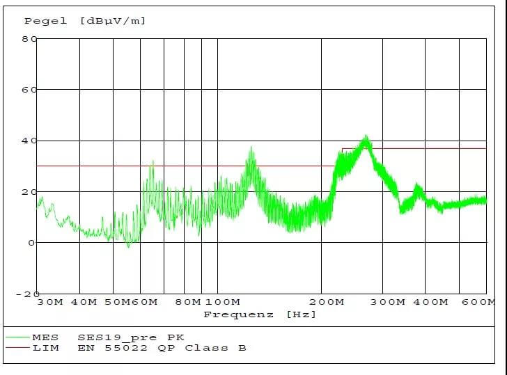
Waveform observation using a spectrometer to observe where the problem appears in the spectrum to make it easier to find the problem. In addition, some low-frequency circuit design habits need to be noted. For example, single-point grounding is perfect for low-frequency applications and not for RF signal occasions, where there are more EMI problems.
Some engineers will apply single-point grounding to all product designs without recognizing that using this grounding method may create additional or more complex EMC problems.
We should also pay attention to the direction of current flow within circuit components. From circuit knowledge, we know that current flows from where the voltage is high to where it is low and that current always flows through one or more paths in a closed-loop circuit, so there is a very important rule: design a minimum circuit.
For those directions where interference currents are measured, the PCB alignment is modified so that it does not affect the load or sensing circuitry. Those applications that require a high impedance path from the power supply to the load must consider all possible paths through which the return current can flow.
We also need to pay attention to the PCB alignment. The impedance of the conductor or alignment contains resistance R and inductance, and at high frequencies, there is impedance and no capacitive resistance.
When the alignment frequency is higher than 100kHz or more, the wire or alignment becomes inductive. A wire or alignment operating above audio may become an RF antenna.
In the specification of EMC PCB design, it is not allowed to operate the wire or alignment below λ/20 of a particular frequency (the design length of the antenna is equal to λ/4 or λ/2 of a particular frequency).
If accidentally designed that way, then the alignment becomes a high-performance antenna, which makes the later debugging more tricky.
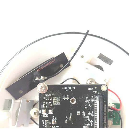
PCB layout of EMC PCB design guidelines
First: consider the size of the PCB. the size of the PCB is too large, with the growth of the alignment to make the system’s anti-interference ability decrease, the cost increases, while the size is too small to easily cause heat dissipation and mutual interference problems.
Second: then determine the location of special components (such as clock components) (clock alignment is best around not laying the ground and do not go up and down in the key signal lines to avoid interference).
Third: based on the function of the circuit, the overall layout of the PCB. In the component layout, the relevant components are as close as possible, so that you can get a better anti-interference effect.