Today, we talk about the EMI PCB design in the PCB design industry, we listed some of the EMI PCB design guidelines.
The most common problem in PCB design is the signal line across the split ground or power supply and EMI problems. To circumvent this EMI problem below to introduce you to the EMI PCB design of PCB design specification steps.
IC power supply processing of EMI PCB design
Ensure that each IC power PIN has a 0.1μF decoupling capacitor, for BGA CHIP, the requirements of the four corners of the BGA are 0.1μF, 0.01μF capacitors a total of 8. Particular attention should be paid to the power supply of the alignment to add filtering capacitors, such as VTT, etc.
This not only has an impact on stability but also has a great impact on EMI. General decoupling capacitors still need to follow the requirements of the chip manufacturer.
Clock line processing of EMI PCB design
- It is recommended to take the clock line first.
- Frequency greater than or equal to 66M clock line, the number of perforations do not exceed 2, the average shall not exceed 1.5.
- Frequency less than 66M clock line, the number of holes per line should not exceed 3, the average shall not exceed 2.5
- The length of the clock line is more than 12inch, if the frequency is greater than 20M, the number of holes shall not exceed 2.
- If the clock line has a hole, in the adjacent location of the hole, the second layer (ground layer) and the third layer (power layer) between the addition of a bypass capacitor, to ensure that the clock line after the layer change, the reference layer (adjacent layer) of the high-frequency current loop continuity.
The power supply layer where the bypass capacitor is located must be the power supply layer through the vias, and as close as possible to the vias, with the maximum distance between the bypass capacitor and the vias not exceeding 300MIL.
- All clock lines must not be islanded (across the split) in principle. Four cases of islanding are listed below.
Clock, reset, signals above 100M, and some critical bus signals cannot cross the split with at least one complete plane, preferably the GND plane.
Clock signals, high-speed signals, and sensor signals are prohibited across the split.
Differential signals must be balanced to the ground to avoid a single line across the split. (Try to cross split vertically)
The high-frequency return path of all signals is located directly below the signal line of the adjacent layer. Signal integrity and timing issues can be significantly reduced by having a solid layer below the signal that provides a direct loop for that signal.
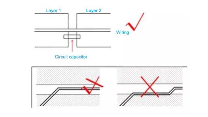
A 0.01 uF loop capacitor should be used when the crossover of the alignment and layer split is unavoidable. When using a loop capacitor, the loop capacitor should be arranged as close as possible to the intersection of the signal line and the layer split as shown in Figure.
6.1. Cross-islanding occurs between the power island and the power island. In this case, the clock line is aligned on the back of the fourth layer, the third layer (power layer) has two power islands, and the alignment of the fourth layer must cross these two islands.
6.2. Cross-islands appear between the power island and the ground island. In this case, the clock line in the fourth layer of the back of the alignment, the third layer (power layer) of a power island in the middle of a ground island, and the fourth layer of the alignment must cross these two islands.
6.3. Across the island appears between the ground island and the ground layer. In this case, the clock line is routed on the first layer, the second layer (ground layer) has a ground island in the middle, and the alignment of the first layer must cross the ground island, which is equivalent to the ground line being interrupted.
6.4. The clock line is not laid under the copper. If the conditions really cannot do without islanding, to ensure that the frequency is greater than or equal to 66M clock line does not wear islanding, frequency less than 66M clock line if the island, you must add a decoupling capacitor to form a mirror path. Between the two power islands and near the cross-island clock line, place a capacitor of 0.1UF.
- When faced with the trade-off between two vias and one islanding, choose one islanding.
- The clock line should be far away from the I/O side of the board edge more than 500MIL, and do not and I/O lines and walk, if you really cannot do, the clock line and I/O port line spacing should be greater than 50MIL.
- clock line to go in the fourth layer, the reference layer of the clock line (power plane) should be as far as possible for the clock power supply surface, the other power surface for the reference clock the less the better, in addition, the frequency is greater than or equal to 66M clock line reference power surface must be 3.3V power plane.
- Clock line hitting when the line spacing should be greater than 25MIL.
- The clock line hitting the line in and out of the line should be as far as possible. Try to avoid similar to Figure A and Figure C show the way to hit the line, if the clock line needs to change the layer, avoid using Figure E of the way to hit the line, using Figure F of the way to hit the line.
- clock line connected to BGA and other devices, if the clock line for layer, try to avoid using Figure G alignment form, over-hole do not go under the BGA, the best use of Figure H alignment form.
- Pay attention to each clock signal, do not ignore any of the clocks, including AUDIO CODEC AC_BITCLK, pay particular attention to FS3-FS0, although it is not a clock from the name, but actually running the clock, to be noted.
- Clock Chip pull-up pull-down resistor as close as possible to the Clock Chip.
I/O port handling of EMI PCB design
- Each I/O port including PS/2, USB, LPT, COM, SPEAK OUT, GAME is divided into a piece of ground, the leftmost and rightmost connected to the digital ground, the width is not less than 200MIL or three over-hole, other places do not connect to the digital ground.
- If the COM2 port is pin type, as close as possible to the I/O ground.
- I/O circuit EMI devices as close as possible to the I/O SHIELD.
- I/O port at the power supply layer and the ground layer of a separate island, and Bottom and TOP layer are to lay the ground, no signal through the island (signal lines pulled directly out of the PORT, not in the I/O PORT in a long distance to go).
A few EMI PCB design notes
- EMI PCB design specifications, design engineers to strictly comply with, EMI PCB design engineers have the power to check, contrary to EMI PCB design specifications and lead to EMI test FAIL, the responsibility of the design engineer.
- EMI PCB design engineers are responsible for the design specifications, strict compliance with EMI PCB design specifications, but still, EMI test FAIL, EMI PCB design engineers have the responsibility to give solutions and summarize the EMI PCB design specifications.
- EMI PCB design engineers are responsible for each peripheral port EMI test, cannot miss the test.
- Each PCB design engineer has the right to make changes to the design specifications and the right to question. EMI PCB design engineers have the responsibility to answer the question, the engineer’s proposal through the experiment after confirmation into the EMI PCB design specifications.
- EMI PCB design engineers have the responsibility to reduce the cost of EMI PCB design, reduce the number of magnetic beads used.