First, the PCB board concept
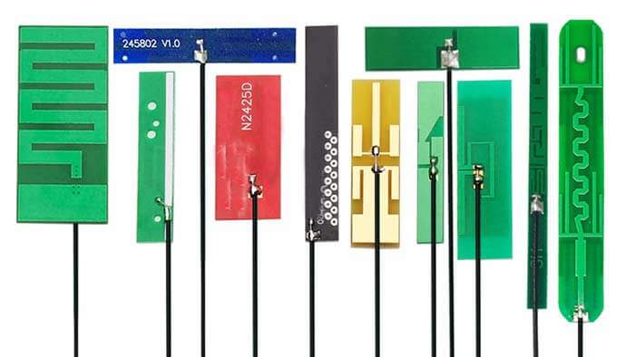
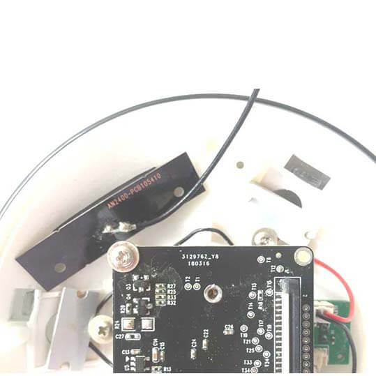
PCB board also known as the printed circuit board, is an important electronic component, is the support body of electronic components, and is the provider of electrical connection of electronic components. As it is made using electronic printing, it is called a “printed” circuit board.
A printed circuit board(PCB) is a laminated sandwich structure of conductive and insulating layers.
Second, the role and function of PCB board in various electronic devices
PCB board Pad
To provide integrated circuits and other electronic components fixed, mechanical support for assembly.
PCB board alignment
PCB board wiring and electrical connections between various electronic components such as integrated circuits (signal transmission) or electrical insulation. Provide the required electrical characteristics, such as characteristic impedance, etc.
PCB board green oil and screen printing
To provide automatic assembly of the solder resist graphics, for component insertion, inspection, maintenance to provide identification characters and graphics.
Third, PCB board technology development summary
From 1903 to the present, if the application of PCB assembly technology and development perspective, can be divided into three stages.
Through-hole insertion technology (THT) stage PCB
The role of metalized holes.
(1). Electrical interconnection – signal transmission
(2). Support components — pin size limits the size of the through-hole reduction
a.Rigidity of the pins
b.Requirement of automated insertion and assembly
Ways to improve density
(1) reduce the size of the device hole, but by the rigidity of the component pins and the limitations of the insertion accuracy, hole diameter ≥ 0.8 mm
(2) reduce the line width / spacing: 0.3mm, 0.2mm, 0.15mm, 0.1mm
(3) increase the number of layers: single-sided, double-sided, 4 layers, 6 layers, 8 layers, 10 layers, 12 layers, 64 layers
Surface mount technology (SMT) stage PCB conductive hole role.
Only to play the role of electrical interconnection, the aperture can be as small as possible, and the plug of the hole can also be.
The main way to improve the density
(1). Dramatic reduction in the size of the through-hole: 0.8mm-0.5mm-0.4mm-0.3mm-0.25mm
(2). The structure of the perforation changes essentially.
a. Buried blind hole structure advantages:
Improve the wiring density by more than 1/3, reduce the size of the PCB or reduce the number of layers, improve reliability, improve the characteristic impedance control, reduce crosstalk, noise, or distortion (due to short lines, small holes)
b. Hole in pad (hole in pad) eliminates relay holes and connecting lines
(3) Thinness: double panel: 1.6mm,1.0mm,0.8mm,0.5mm
(4) PCB flatness.
a. Concept: PCB board substrate warpage and the coplanarity of the surface of the connection plate on the PCB board surface.
b. PCB warpage is due to thermal and mechanical residual stress caused by the combined results
c. Surface coating of the connection plate: HASL, chemical plating NI/AU, electroplating NI/AU.
Chip-level packaging (CSP) stage PCB
CSP began to enter a dramatic change in the development of PCB technology to promote the continuous development of the PCB board industry will move toward the laser era and the nano era.
Fourth, PCB board surface coating technology
PCB board surface coating technology refers to the solder resist coating (and protection) layer other than the power supply gas connection with a solderable coating (plating) layer and protective layer.
PCB board classification by application
- For soldering: Because the surface of copper must be protected by a coating layer, otherwise, it is easily oxidized in the air.
- For connectors: electroplated Ni/Au or chemically plated Ni/Au (hard gold, containing P and Co)
- For wire bonding: wire bonding process
Hot air leveling (HASL or HAL)
The PCB from the molten Sn/Pb solder is blown flat by hot air (230°C).
Basic requirements
(1). Sn / Pb = 63/37 (weight ratio)
(2). Coating thickness at least >3um
(3) to avoid the formation of non-solderable Cu3Sn, Cu3Sn appears due to insufficient tin, such as Sn/Pb alloy coating layer is too thin, the composition of the solder joint from the solderable Cu6Sn5 – Cu4Sn3 – Cu3Sn2 – non-solderable Cu3Sn
Process flow
Removal of resist – board cleaning – printing of solder resist and characters – cleaning process – flux coating – hot air leveling – cleaning process
Disadvantages
a. Lead tin surface tension is too large, easy to form the turtleback phenomenon.
b. The pad surface is not flat, which is not conducive to SMT soldering.
Chemical plating Ni / Au is the PCB board connection plate chemically plated Ni (thickness ≥ 3um) and then plated with a layer of 0.05-0.15um thin gold, or plated with a thick layer of gold (0.3-0.5um). Because of the chemical plating uniform, coplanar good, and can provide multiple welding performance, therefore has the trend of promoting the application. Plating thin gold (0.05-0.1um) is to protect the Ni solderability, and plating thick gold (0.3-0.5um) is for wire bonding (wire bonding) process needs.
The role of the Ni layer
a. As Au, Cu between the isolation layer, to prevent them from spreading between each other, resulting in its diffusion parts are loose state.
b. As a weldable layer, the thickness of at least > 3um
Role of Au
Au is the protective layer of Ni, thickness between 0.05-0.15, cannot be too thin, because the gold porosity is larger if too thin cannot be well protected Ni, resulting in Ni oxidation. Its thickness cannot be > 0.15um, because the solder joint will form a gold-copper alloy Au3Au2 (brittle ), when the solder joint Au is more than 3%, the weldability becomes poor.
Electroplated Ni/Au
The plating structure is basically the same as chemical Ni/Au, because of the use of electroplating, the uniformity of the plating is less.
Fifth, PCB design output production files Notes
- The layers to be output is:
(1). Wiring layers including top/bottom/intermediate wiring layers.
(2). Screen printing layer including the top screen printing/bottom screen printing.
(3). Solder resist layer including top layer solder resist and bottom layer solder resist.
(4). Power supply layer including VCC layer and GND layer.
(5). In addition, the drill file NCDrill is generated.
- If the power layer is set to Split/Mixed, then select Routing in the Document item of the document window and use PourManager’s plane connect to clad the PCB board before outputting the light painting file each time; if it is set to CAMPlane, then select Plane in the When setting the Layer item, add Layer25 and select Pads and Vias in Layer25.
- In the Device Setup window, press Device Setup and change the value of Aperture to 199.
- Select Board Outlines when setting the Layer for each layer.
- When setting the Layer of the screen printing layer, do not select Part Type to select the top-bottom layer and Outline Text Line of the screen printing layer.
- When setting the Layer of the solder resist layer, select Over Hole to indicate that no solder resist is added to the over hole. Generally, the over hole will be covered by the group solder layer.
Sixth, PCB board safety marking requirements
- The PCB board safety marking of the fuse is complete whether there are 6 complete markings near the fuse, including fuse serial number, fusing characteristics, rated current value, explosion-proof characteristics, rated voltage value, and English warning mark. Such as F101 F3.15AH,250Vac, “CAUTION: For continued protection Against Risk of Fire, Replace Only With SameType and Rating of Fuse “. If there is no space on the PCB board to line up the English warning labels, you can put the work, English warning labels into the product instructions.
- PCB board on the dangerous voltage area marked with high-voltage warning symbol PCB dangerous voltage area part of the application of 40mil wide dotted line and the safety of the voltage area isolation, and printed on the high-voltage danger signs and “DANGER! HIGH VOLTAGE”.
- The originally paid side of the isolation zone clearly marked PCB’s original, paid side of the isolation zone is clear, with a dotted line in the middle of the mark.
- PCB board safety markings should be clear and complete.


